
Microfluidic flow cells are transforming diagnostics by enabling simultaneous detection of multiple biomarkers in a single assay. Discover in the second part of our four-part series how to successfully navigate the development process. Our comprehensive article covers design, material selection, and manufacturing methods for thermoplastic and glass-based microfluidic devices.
Our next article will provide in-depth information on 3D printing, soft lithography, lateral flow manufacturing, and how to choose your manufacturing pathway.
Overview
Microfluidic flow cells have emerged as a transformative force driven by advancements in life sciences and diagnostics. With a growing variety of materials and manufacturing techniques, choosing the right fabrication path can be as critical as the design itself. Exploring key manufacturing methods, their advantages and challenges, and how they align with application needs ensures functional, reproducible, and cost-effective devices.
Design for manufacturing
Why design tools and rules come first
Microfluidic chips are not just scaled-down “plumbing systems”. Channel cross-sections, surface energies, wall elasticity, and even polymer birefringence steer the physics. Therefore, a layout that works on a whiteboard can fail catastrophically once it is applied to real materials and processes.
Although the list is long, you should consider the parameters that influence fluid behavior within microfluidic channels when utilizing such simulation tools (see table below).
|
Category |
Key parameter(s) |
Why it matters |
Typical dimensionless group(s) |
Example |
|
Geometry |
Channel width/height/length, aspect ratio, bends/curvature, surface roughness, or patterns |
Sets hydraulic resistance, shear-rate profile and secondary flows (Dean vortices in curves). Smaller Dh lowers Re. |
Reynolds Re, Dean De |
Organ-on-a-chip serpentine vs. straight layouts |
|
Surface and Wettability |
Hydrophilicity/ hydrophobicity (contact angle), surface energy; surface charge (ζ-potential); coatings; nano-texture; elastic compliance |
Controls capillary pressure, slip/no-slip behavior, bubble nucleation, wetting patterns and electro-osmotic mobility; soft walls deform under pressure and alter cross section. |
Capillary Ca, electric Dukhin Du |
Wettability effects on capillary flow in COC (cyclic olefin copolymer) vs. PDMS (poly-dimethylsiloxane) |
|
Intrinsic fluid properties |
Density ρ; dynamic viscosity μ; surface and interfacial tension γ; diffusivity D; rheology (Newtonian vs. viscoelastic) |
Dictate inertial vs. viscous balance, diffusion vs. advection mixing, droplet breakup/size and particle focusing. |
Re = ρuL/μ, Ca = μu/γ, Peclet Pe, Weissenberg Wi |
T-junction droplet size vs. Ca |
|
Operating conditions |
Volumetric flow rate Q or pressure drop ΔP; temperature; imposed concentration/chemical gradients |
Flow rate sets shear and residence time; heating changes viscosity and reaction kinetics; gradients drive phoresis or chemotaxis. |
Same groups above + Grashof Gr |
Thermal control shifting flow in lab-on-chip |
|
External fields |
Electric (E), magnetic (B), acoustic, optical forces |
Add body forces for pumping, particle manipulation, mixing, droplet merging/splitting without changing channel geometry. |
Electro-osmotic Eλ/μ, Magnetic Mason Mn, Acoustic Strouhal St |
E-field + Re, Ca predicting droplet size |
|
Multiphase specific |
Flow-rate ratio; viscosity ratio; surfactant concentration; interfacial modifiers |
Determine droplet/bubble size, breakup regime, and stability in emulsions or gas–liquid operations. |
Ca, Weber We |
Systematic Ca + flow-ratio droplet maps |
|
Mixing and diffusion |
Channel Re; Pe; chaotic-advection structures (herringbone, zig-zag, serpentine) |
Control homogenization time for reagents, heat, or cells; dominates assay repeatability. |
Pe = µL/D, |
Passive mixer efficiency vs. Pe |
Parameters that influence fluid behavior within microfluidic channels.
Modern micro-CAD and simulation suites are, therefore, upstream of fabrication. They convert performance targets (flow rate, shear, droplet size, particle cut-off, etc.) into geometries that adhere to the constraints of the chosen manufacturing route.
|
Tool/platform |
Main purpose |
|
No-code, browser-based CAD with drag-and-drop channels, real-time flow simulation and direct-to-fab export |
|
|
COMSOL Multiphysics 6.2 – Microfluidics Module |
GPU-accelerated FEM (finite element method) for laminar, two-phase, electro-osmotic and particle tracing; parametric CAD linkage |
|
GPU-accelerated CFD (computational fluid dynamics) (Level-set and VOF) with wizard-driven pre-processing for microchannels |
|
|
VOF-based CFD templates for capillary, droplet optics and microscale mixing; built-in POST visualizer |
|
|
ML-based inverse design: specify performance targets (split ratio, pressure drop) → auto-generate channel network |
|
|
Web-based, PCB-style schematic capture and 3D visualization with extensible component library |
|
|
Evolutionary-algorithm + CFD-surrogate + fab-in-the-loop for rapid droplet device design |
|
|
Multi-objective optimizer for deterministic lateral displacement devices (pillar geometry → critical diameter) |
|
|
SPICE-like netlist for 1-D flow models linked to high-level synthesis; open-source C++ library |
|
|
CNN + reinforcement learning for droplet path labeling and optimized electrode actuation |
Overview of CAD and simulation suites.
It is important to know what you want to achieve when using simulation programs.
Rapid CAD-to-FAB tools (e.g., Flow Circuits) excel at geometry layout and simple flowrate checks but do not model surface wetting, complex fluids, fields, or droplets. These are meant for DFM (design for manufacturing) and quick prototyping rather than deep physics. Full-physics CFD packages (COMSOL, ANSYS, and FLOW-3D) cover all categories: geometry, fluid properties, operating conditions, external fields, multiphase, and mixing.
Consequently, in a commercial environment, the focus must be on utilizing rapid CAD-to-FAB-tools to cover the major design challenges while reserving the complex full-physics CFD tools to address critical obstacles and specific assay challenges later in the development process.
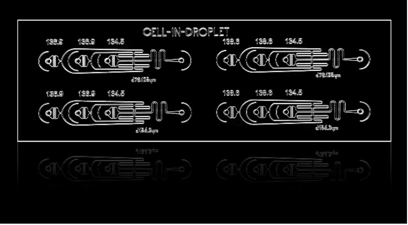
Glass flow cell enabling production of double emulsion droplets incorporating individual cells.
Photo courtesy of IMT Microtechnologies, Switzerland).
Choose the right material for your application
The material affects performance, compatibility, and manufacturability
Initially, silicon- and glass-based substrates dominated as efficient materials for microfluidic devices. In a landmark paper, Manz et al. 1990 proposed combining classical analytical functions – sample injection, separation (capillary electrophoresis or liquid chromatography), and detection – onto a single silicon/glass chip, spearheading the “lab-on-a-chip” era.
Comparison of manufacturing techniques for microfluidic chips
(from Materials for Microfluidic Chip Fabrication
by Ren et al. 2013 Accounts of Chemical Research 46(11)2396–2406.).
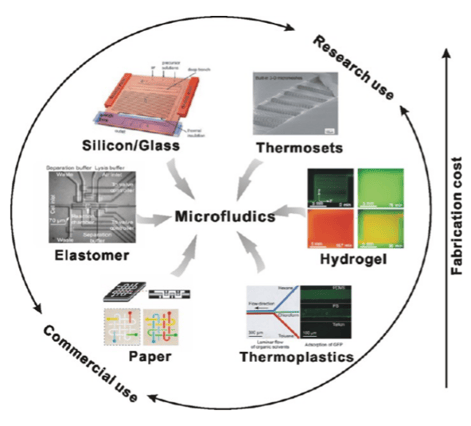
However, as microfluidic technology developed, other materials also gained importance for evaluation as microfluidic materials. Microfluidic materials are broadly divided into three major types: inorganic materials, polymeric materials, and paper. Ceramic materials are included in the inorganic materials category, along with silicon and glass materials. Thermoplastics and elastomers are the main classes of polymeric materials. Microfluidic paper-based systems fundamentally differ from inorganic and polymeric structures in that they are typically open, whereas the classical systems are closed except for specific inlet and outlet ports.
The Microfluidics Association has published a series of white papers that outline best-practices for producing microfluidic solutions, including detailed guidelines on design and fabrication. The MFA is continually expanding these resources—developing more comprehensive guidelines and standards through our workshops and via the MFA-supported ISO working group. For access to the latest documents, visit https://microfluidics-association.org/downloads/.
It is important to select the materials for microfluidic-device fabrication based on device function, intended use, cost target, and degree of integration. In addition to these factors, the fabrication process along with the physical properties of materials such as electrical and thermal conductivity, flexible nature, absorptivity, optical transparency, air permeability, and compatibility with solvents should be considered. The most important materials used in microfluidic devices are summarized in the table below.
|
Material |
Channel dimension |
Working temperature [°C] |
Compatible solvents |
Fabrication methods |
|
Silicon |
<100 nm |
<1415 |
Most solvents, no KOH |
Wet-, dry-etching |
|
Glass |
~10 µm |
<600 |
Most solvents, no HF |
Wet-, dry-etching |
|
Elastomer |
<1 µm (3D) |
Medium |
Less solvent compatible |
Costing |
|
Thermoset |
<100 nm |
High |
High solvent compatible |
Casting, Photopolymerization |
|
Thermoplastics |
~10 µm |
High |
Good solvent compatible |
Thermomolding |
|
PDMS |
~20 nm |
<40–50 |
No most organic solvents |
Casting |
|
Polycarbonate |
~100 nm |
<125 |
No KOH, ketones, acetone |
Thermomolding |
|
Hydrogel |
~10 µm |
<25–32 |
No most solvents |
Casting; Photopolymerization |
|
Polyimide |
<100 nm |
<400 |
Most solvents |
Casting; Photopolymerization |
|
SU-8 photoresist |
<100 nm |
<150 |
Most solvents |
Casting; Photopolymerization |
|
Perflouroakoxy (Teflon PFA) |
~100 nm |
<260 |
Most solvents |
Thermomolding |
|
Fluorinated ethylenepropylene (Teflon FEP) |
~100 nm |
<200 |
Most solvents |
Thermomolding |
|
PMMA |
~100 nm |
<60–100 |
No alcohol, acetone, benzol |
Thermomolding, 3D printing |
|
Paper |
~200 µm |
<30–50 |
No organic, surfactant solvents |
Etching, printing |
Summary of the common materials used in microfluidic devices
(from Development of glass-based microfluidic devices: A review on its fabrication and biologic applications by Aralekallu et al. 2023, Materials & Design: 225, 111517).
Select the materials for microfluidic-device fabrication based on device function, intended use, cost target, and degree of integration.
Thermoplastic microfluidic manufacturing processes
Advantages and challenges of the methods
Manufacturing microfluidic devices for multiplex detection involves several advanced techniques, each presenting unique benefits and challenges. It is crucial to ensure efficient, high-yield production while maintaining the integrity and functionality of the devices.
1. Injection molding
Injection molding is ideal for large-scale production of thermoplastic microfluidic devices. Molten material is injected into a mold to form the desired structures.
Advantages:
- Scalability: Offers high precision and rapid production cycles, making it suitable for mass manufacturing.
- Material flexibility: The wide range of polymer materials and additives available on the market allow for optimization of material and surface properties to the intended applications. While the injection behavior of polymers can vastly differ, it is often still feasible to switch materials even after the molds have been generated.
Challenges:
- Cost: High initial costs for mold fabrication need to be considered.
- Design flexibility: Once molds are created, making design changes is costly and time-consuming, reducing flexibility.
- Sealing: While the molding process itself can be extremely accurate, sealing the chips may limit channel precision and feature size and drives up the per-chip cost. Additionally, thin adhesive top-layers sets limits to the applicable pressure ranges.

Cross flow Membrane Chips with integrated Mini Luer Connectors. |
A number of companies offer expert services for providing injection-molded microfluidics devices. See the overview below.
|
Company |
Injection molding service |
|
|
ThinXXS Microtechnology |
Multi-shot (2-K) injection-molded cartridges with integrated pumps/valves; turnkey design-to-scale manufacturing |
|
|
(formerly MiniFAB) |
ISO-clean-room micro-injection molding, blister integration & automation for IVD cartridges |
|
|
Microfluidic ChipShop |
Fast aluminum tooling for COC/COP, PMMA, PC; scales to multi-cavity steel molds |
|
|
(Enschede, Netherlands) |
Hybrid glass & polymer chips; in-house pilot injection-molding line for thermoplastics |
|
|
(Eindhoven, Netherlands) |
Ultra-precision mold making and micro-injection molding/bonding of diagnostic cartridges |
|
|
(ex-Sony DADC) (Anif, Austria) |
Optical-disc heritage → very high-volume molding, solvent/laser welding & coating of microfluidics |
|
|
(Roding, Germany) |
Medical-grade micro-injection molding of cartridges with 10 µm-scale channels |
|
|
(Toronto, Canada) |
Rapid aluminum tools, proprietary bonding; bridge-to-production volumes in COC, PMMA, PC |
|
|
(Molex) |
Large-scale molding & automated assembly for IVD and drug-delivery microfluidic parts |
|
|
Class-6 clean-room injection molding, in-house tool shop, automated assembly & bonding |
||
|
(Mondragón, France) |
Combines MEMS photolithography with micro-injection molding for polymer chips |
|
Overview of providers of injection molding services.
Hot embossing and injection molding both replicate thermoplastic microfluidics from mold inserts, but they occupy different positions on the cost-versus-volume curve. A common product roadmap is emboss → pilot validation → scaling in injection molding, re-using master designs and surface chemistries while trading longer cycle times for the ultra-low unit costs achievable with high-cavity injection tools (Scott and Ali 2021, Attia et al. 2009, and Liu et al. 2024).

|
Illustration of the fabrication methods currently used in microfluidics: replica molding, injection molding, and hot embossing
(from Manufacturing of 3D-Printed Microfluidic Devices for the Synthesis of Drug-Loaded Liposomal Formulations
by Ballacchino et al. 2021 Int. J. Mol. Sci. 22(15), 8064).
2. Hot embossing
Hot embossing is a replication method in which a thermoplastic substrate is heated – often in a vacuum to ensure uniform temperature – and then pressed against a master mold containing the inverse microstructures. Under controlled temperature and pressure, the softened polymer conforms to the mold’s features and, upon cooling, retains these high-fidelity details with minimal residual stress. This method is particularly effective for moderate-volume production where the replication of nanoscale features is critical, as it benefits from lower thermal cycles compared to melting-based techniques. In contrast, injection molding involves melting the thermoplastic completely and forcefully injecting it into a precision-engineered mold cavity at high pressure. This process enables rapid cycle times and is ideal for high-volume production, but it requires a substantially higher initial investment in mold fabrication. The high-pressure injection can also induce greater residual stresses and potential warpage, which may necessitate post-processing to achieve the desired surface quality and dimensional accuracy.
Comparatively, hot embossing operates at lower pressures and with a reduced thermal cycle, thereby minimizing internal stresses and achieving finer feature resolution. Recent advances, such as ultrasonic hot embossing, further improve process speed by localizing the heating process, thereby reducing cycle times while still maintaining high replication fidelity. Ultimately, the choice between injection molding and hot embossing depends on the balance between production scale, cost constraints, and the need for precise microstructural features in microfluidic device applications.
|
Company |
Hot-embossing service |
|
Microfluidic ChipShop |
Offers polymer replication by injection molding, hot embossing, or casting for rapid prototypes and scale-up of lab-on-a-chip devices |
|
Potomac Photonics |
Job-shop micro-fabrication; hot-embosses COC, PMMA and other plastics to deliver cost-effective microfluidic parts from prototypes to pilot batches |
|
Hahn-Schickard |
“Micro-thermoforming / hot-embossing” line for low-tool-cost functional models and proof-of-concept microfluidic films & plates |
|
uFluidix |
Uses hot embossing when sub-10 µm fidelity is required in thermoplastics; integrates bonding & finishing for pilot volumes |
|
Temicon GmbH (Dortmund & Freiburg, Germany) |
Large-area roll-to-plate nano-/micro-replication; supplies nickel shims and hot-embossed polymer sheets with microfluidic patterns |
|
Axxicon |
ISO-13485 tool-maker; offers hot embossing (alongside injection molding) for rapid microfluidic consumable prototypes before scaling |
Overview of providers of hot embossing services.
Parallel Fluidics in Boston, MA offers an innovative on-demand prototyping service for microfluidic devices using thermoplastics, delivering production-grade prototypes within one week. Their “Transition Molding” process combines the quality and performance of injection molding with the rapid turnaround and low-volume flexibility needed in the early stages of product development.
It’s crucial to ensure efficient, high-yield production while maintaining the integrity and functionality of thermoplastic microfluidic devices.
Glass and Si-based microfluidic manufacturing processes
|
Suitable for high-performance diagnostic and research applications Glass-based microfluidics are highly regarded for their optical clarity, chemical resistance, thermal conductivity, and biocompatibility. These systems are particularly suitable for high-performance diagnostic and research applications. Key fabrication techniques include wet or dry etching, and bonding methods such as anodic bonding, each tailored for specific applications. |

Fabrication techniques for glass-based microfluidics |
- Wet etching: This process involves chemical etching using solutions like HF to create channels and structures on glass substrates. It provides high-quality surface finishes but lacks the resolution of dry etching.
- Dry etching: Methods like deep reactive ion etching (DRIE) are used to produce intricate microstructures with excellent precision. This technique is preferred for applications requiring sub-micron features.
- Laser ablation: Recent innovations have seen the use of laser ablation for rapid prototyping of glass microfluidic devices but also to generate access holes to the microfluidic channels (ROFIN, LightFab, 3D-Micromac, and Corning Laser Technologies). This approach allows for the direct fabrication of channels without masks, reducing production time while maintaining precision. See the table below for a list of specialist providers offering laser-based glass micromachining – drilling, ablation, selective etching – for microfluidic applications. This selection spans job-shop service bureaus (GFH, 3D-Micromac, and Potomac), foundries with in-house research and development (IMT AG and FEMTOPRINT), and institutional partners (Fraunhofer) who push selective laser-etching and ultrafast laser processes for both prototyping and small-series production of glass microfluidic components.

Image of isotropically etched channels in a glass substrate, courtesy of Micronit, NL.
|
Company |
Service |
|
GFH GmbH |
Ultrashort-pulse laser micromachining (drilling, cutting, engraving) of glass with micron-scale precision |
|
LightFab |
Selective Laser-Induced Etching (SLE) for through-holes, internal channels & 3D structures in fused silica |
|
3D-Micromac AG |
Industrial laser micromachining (µ-drilling, structuring) on glass substrates |
|
Potomac Photonics |
Precision laser drilling of glass slides & coverslips for microfluidic ports and vias |
|
IMT AG |
Glass wafer processing with laser-assisted etching to define vertical interconnect holes for 3D channel networks |
|
FEMTOPRINT SA |
Ultrafast laser–based 3D micro-manufacturing platform for prototyping functional glass microdevices |
|
Fraunhofer ILT/IPT |
R&D & pilot-scale laser processes (SLE, micro-ablation, welding) for bespoke glass microfluidic systems |
Overview of providers of laser ablation services.
Glass and Si-based systems are particularly suitable for high-performance diagnostic and research applications.
Copy of the first miniaturized µTAS glass flow cell of Manz et al.
Photo courtesy of IMT Microtecnologies AG, Switzerland.
Practical advice before you start
- Ask about hybrid approaches
Even if a manufacturer does not offer a “pure” laser bond, they may combine laser pre-bonding steps with low-temperature thermal finishing, or use lasers for localized sealing. - Evaluate volume and cost
Laser-based bonding can be more expensive and slower than furnace-based fusion for high-volume runs, but it can be ideal for localized bonding, delicate structures, or where you need to avoid exposing the entire wafer to high temperatures. - Leverage R&D partners
Many advanced bonding techniques originate in research labs or institutes. If commercial providers aren’t publicly advertising laser bonding, consider a joint development project with an R&D institute (like Fraunhofer) or approach your existing manufacturer about the feasibility of a custom laser-bonding process. - Check patents and publications
Laser-based glass welding for microfluidics is still developing. Scouring patent databases or recent technical publications can reveal new players, specialized startups, or labs offering partnership opportunities.
 Silicon-Glass microfluidic device utilizing anodic bonding, courtesy of Micronit, NL.
Bonding for Si-glass integration
Several techniques can be applied to provide a robust seal for all-silicon, all-glass, or silicon-glass microfluidic devices. Anodic bonding creates robust seals between silicon and glass substrates with bonding strength higher than the material breaking strength. This method ensures high chemical resistance and thermal stability, making it ideal for applications involving aggressive reagents or high-temperature processes.
|
Its drawback is the requirement for high temperatures, i.e., >550°C. This does not facilitate integration of binding or other chemistry in the channel network. Alternatives are readily available such as wafer level adhesion bonding, utilizing biocompatible adhesives. Laser based bonding is also successfully utilized in the industry, in combination with polymer intermediary layers providing the microfluidic network, e.g., Illumina Flow Cells, hybrid glass plastic flow cell and fabrication methods. Another possibility is glass–glass bonding, e.g., the SCHOTT Primoceler, which can potentially offer low-temperature bonding. |

Glass flow cell with integrated electrodes to perform impedance measurements. Bonding facilitated by a structured intermediary layer. |
Challenges and solutions
While glass-based devices offer unparalleled performance, the misconception of having high fabrication costs and brittle substrates persists. The commercial success of several platforms contradicts the argument, in particular when considering the numbers of measuring points per surface performed in such flow cells. Also, initial costs for a glass flow cell are lower compared to injection molded parts. The financial advantage of glass flow cells can be sustained well up to 100k units p.a. though for high-volume consumables injection molding should be the material of choice (Yole Group 2019).
Applications and industry adoption
Companies like IMT Masken und Teilungen, Micronit, little things factory, and imec are leaders in providing advanced glass-based microfluidic solutions. These platforms are used in nucleic acid testing, environmental monitoring, and more.

All-glass flow cell incorporated in a flow-cell carrier for easy system interfacing (from icIEF-UV/MS Technology, of SCIEX an Danaher Company). |
Glass-based microfluidics are also central to cutting-edge applications such as fluorescence imaging and electrochemical sensing, droplet generation for a variety of applications, impedance-based cytometry, e.g., Amphasys, leveraging their transparency and inertness for optimal performance, higher dielectric constant (glass is an excellent isolation material) as well as thermal conductivity for electrophoretic applications (Sciex). |
Comparison of microfluidic chip manufacturing costs
A) Glass/silicon-based microfluidic chips (200 mm wafer, 2 wafers per chip)
Assumptions:
- Wafer diameter: 200 mm
- Chip size: 15 × 15 mm (225 mm²)
- Chips per wafer: ~100 (after accounting for edge losses and spacing)
- 2 glass wafers per device: 2 × $25 = $50/wafer set
- Cleanroom processing cost: $200/wafer set
Cost breakdown per chip:
|
Component |
Estimated $/chip |
|
Material + mask |
$0.60 |
|
Cleanroom processing |
$2.00 |
|
Bonding and dicing |
$2.00 |
|
QC (inspection) |
$0.75 |
|
Direct cost
|
$5.35 |
|
+ R&D / regulatory (40%) |
$2.14 |
|
+ Reseller margin (25%) |
$1.87 |
|
Estimated sale price |
$9.36 |
B. Thermoplastic-based microfluidic chips
Assumptions:
- Mold size: 100 × 100 mm
- Chip size: 15 × 15 mm
- Chips per cycle: ~40
- Mold amortized over 1 million chips
- Resin cost: $5–10/kg (~0.5 g per chip)
Cost breakdown per chip:
|
Component |
Estimated $/chip |
|
Material + tooling |
$0.15 |
|
Processing (molding) |
$0.15 |
|
Bonding and ports |
$0.40 |
|
QC (inspection) |
$0.40 |
|
Direct cost
|
$1.10 |
|
+ R&D / regulatory (40%) |
$0.44 |
|
+ Reseller margin (25%) |
$0.39 |
|
Estimated sale price |
$1.93 |
The essence of this article
Missed the first part of this series?
Read Alexis’ insightful introduction: "Microfluidics in Focus: Benefits and Breakthroughs".
Don't miss the next part of this blog series. Follow us on LinkedIn and be the first to hear about it!
We support your success
As a global systems engineering provider with a proven track record in life science and diagnostics, we recognize your need for innovative solutions. Our deep microfluidics expertise, combined with a full understanding of your workflows, enables us to transform your vision into market-ready solutions that exceed customer expectations.
Contact us and discover how we can help you innovate faster and smarter.

Microfluidics Expert Alexis Tzannis
Alexis holds a PhD in physical chemistry from ETH Zürich, is fluent in four languages, and has a proven record of forging academia–industry partnerships to accelerate innovation. A founding member of the Microfluidics Association (MFA), he is a micro- and nanotechnology business leader with 15 years of experience taking microfluidic products from concept to industrialization.
Alexis has delivered double-digit sales growth at HSE•AG and previously at IMT Microtechnologies by leading cross-functional teams and cultivating global key accounts. His technical expertise spans the design and manufacture of glass, silicon, and hybrid-material microfluidic platforms that enable cutting-edge analytical applications, e.g., next-generation sequencing (NGS) and others.