
The field of microfluidics has revolutionized the handling of liquids on the microscale enabling the development of cost-effective portable devices. Discover in the final part of our four-part series how to select and optimize structured surface functionalization methods. This article provides everything you need to know about the range of methods available, how to create sub-micron spots for analyte capture, challenges and solutions, and more.
Overview
Structured functionalization uses advanced techniques to precisely engineer the surface of the microfluidic device with microscale or even sub-micron capture sites. This allows close control of the surface chemistry and significantly improves efficiency, specificity, speed and throughput in genomics, proteomics, and clinical testing. This level of structured functionalization can be achieved using a variety of techniques, but it is important to take into account the challenges, considerations, and solutions.
An essential requirement in advanced biosensing, diagnostics, and microfluidic applications is the ability to capture a variety of analytes by creating structured surface functional sites of (sub-)micron size, each bearing different capture chemistries. Achieving such precision allows for multiplexed detection of analytes with high sensitivity and specificity. Various methods, often combining multiple techniques, have been developed to accomplish this level of detail in surface functionalization.
Surface functionalization methods
Silanization
Silanization modifies substrate surfaces (e.g., glass, silicon, quartz) with organosilane reagents. These reagents, such as APTES (3-Aminopropyl)triethoxysilane, introduce functional groups (e.g., –NH₂, –SH, epoxy) by forming Si–O–Si bonds with the substrate. This forms a stable, reactive surface for subsequent bioconjugation, for instance for antibody immobilization (Wang et al. 2021).
Silanes for biomolecule immobilization:
-
-
Provide primary amine groups for covalent coupling via EDC/NHS chemistry.
-
Useful for DNA and protein immobilization.
-
2. Epoxysilanes:
-
-
Enable nucleophilic reactions with biomolecules containing amines, thiols, or hydroxyl groups.
-
3. Thiolsilanes and maleimidosilanes:
-
-
Facilitate binding of thiol-containing molecules, such as cysteine residues or thiolated DNA.
-
PEGylation
PEGylation involves the application of polyethylene glycol (PEG) to surfaces to:
- Reduce non-specific binding.
- Enhance biocompatibility.
- Create a hydrophilic, anti-fouling surface for sensitive biomolecule applications, e.g., priming (BOC Sciences).
SuSoS of Switzerland has created a compelling list of surface-related topics for “Bonding anything to anything” that is definitely worth taking a look at.
SuSoS, AziGrip4™, and PAcrAm™ coatings provide highly durable non-fouling surfaces that prevent unspecific protein, cell, and biofilm attachment. These coatings form a stable hydrostatic barrier without using active agents, reducing background noise in diagnostics, improving organoid formation, and preventing clogging or contamination in microfluidics and bioreactors.
The polymeric layers withstand extreme pH, mechanical stress, ethanol, and even γ-sterilization, making them ideal for applications such as organ-on-chip platforms, 3D cell culture, and point-of-care diagnostics.
Formation of spheroids in special wells coated with AziGrip4™ EX.
Copyrights with the copyright holder (from SuSoS Functional Coatings Overview).
PEGylation as an alternative to silanization
- Direct PEGylation: Application of PEG coatings for non-specific binding reduction (BOC Sciences).
- Patterned PEGylation: Use of biotin-PEG or azide-PEG with lithographic techniques for localized functionalization.
Click chemistry
Click chemistry offers a highly efficient and specific method for attaching biomolecules to surfaces. It typically employs copper-catalyzed azide-alkyne cycloaddition (CuAAC), creating stable triazole linkages. This technique is particularly effective for modifying silanized or PEGylated surfaces, enabling precise and stable functionalization (Barua et al. 2021, SuSoS, Switzerland).
Click chemistry for functionalization
- Silanized Surfaces: Functionalize silanized substrates with azide or alkyne groups for subsequent click chemistry reactions (Wang et al. 2021).
- PEGylated Surfaces: Conjugate alkyne-PEG to azide-modified surfaces, achieving both specificity and anti-fouling properties (BOC Sciences).
Protocols for surface functionalization
Cleaning and preparation
-
-
Substrate cleaning: Remove contaminants using piranha solution, plasma treatment, or ethanol washes.
-
Drying: Ensure a dry, clean surface for consistent silanization, PEGylation, or click reactions.
-
Functionalization processes
-
-
Silanization: Apply silane in a controlled solvent or vapor phase, followed by curing at 80–120 °C.
-
PEGylation: Utilize wet-chemistry methods for PEG application, such as spin-coating or immersion (BOC Sciences).
-
Click chemistry: Perform CuAAC reactions to attach biomolecules to azide- or alkyne-functionalized surfaces (Wang et al. 2021).
-
Patterned coatings
-
Photoresist methods: Use lift-off resist (LOR) or photoresist masks for sub-µm patterning.
-
Photoinduced PEGylation: Employ DUV light to pattern azide-PEG coatings for spatially controlled surface modification (BOC Sciences).
Coupling strategies for biomolecules
Structured surface functionalization is crucial in microfluidic devices because it enables precise spatial control of chemical and physical properties within microchannels, directly influencing fluid flow, biomolecule interactions, and detection sensitivity. By patterning hydrophilic and hydrophobic regions or selectively immobilizing biomolecules, devices achieve localized functionality essential for diagnostics, biosensing, and organ-on-chip systems.
For example:
- Aerosol jet printing enables superhydrophobic patterning to control droplet placement.
- Porous silicon photonic chips use spatially defined click-chemistry to allow multiplex protease detection.
- Maskless microplasma techniques create localized wettability contrasts, improving sample confinement in microchannels.
- Non-fouling polymer coatings like SuSoS AziGrip4™ selectively prevent protein and biofilm adhesion in critical sensing regions.
These capabilities improve signal-to-noise ratios, reduce non-specific binding, and allow integration of complex biochemical assays into compact, high-throughput lab-on-chip systems.
DNA and RNA immobilization
Use thiol- or amine-modified oligonucleotides with EDC/NHS, thiol-maleimide, or click chemistries for stable attachment (Barua et al. 2021).
Protein functionalization
Utilize epoxy or amine-functionalized surfaces for covalent binding to lysine or cysteine residues.
Ensure proper orientation with spacers (e.g., PEG) to preserve binding activity. Click chemistry allows stable conjugation of azide-modified aptamers to alkyne-functionalized surfaces (Barua et al. 2021).
Recommendations
- Optimize processes: Address cross-reactions and residue challenges to enhance reproducibility.
- Combine functionalization techniques: Use silane, PEG, and click chemistries synergistically to balance binding specificity and anti-fouling properties (Wang et al. 2021).
- Scale-up potential: Focus on wafer-level integration of patterned coatings for industrial applications (Barua et al. 2021).
Creating structured surface functionalization with (sub-micron-) spots for analyte capture
Combining lithographic techniques, surface functionalization, and CVD for advanced multiplex detection
Advanced biosensing and diagnostics rely on creating structured surface functionalization with ideally sub-micron precision, allowing for the multiplexed detection of analytes with high sensitivity and specificity. Several methods, often integrated, facilitate this precision, each with unique benefits and considerations. These advanced patterning and surface functionalization techniques are commonly employed using substrates like glass or silicon wafers, which offer excellent stability, compatibility, and optical properties.
Integration: Structured Silanization Case Study
Within the context of advanced surface functionalization strategies, the collaborative innovation between IMT and CSEM represents a state-of-the-art demonstration of how structured silanization can be applied to achieve high-performance microfluidic devices.
Despite plastics dominating microfluidic consumables, glass offers unmatched optical clarity, chemical stability, and low autofluorescence, making it ideal for high-sensitivity bioassays. Historically, its use has been limited by high production costs and the risk of damaging pre-immobilized biomolecules during bonding.
Supported by InnoSuisse, IMT AG and CSEM developed a cost-effective wafer-scale manufacturing process that combines:
- Surface microstructuring for precise fluidic geometries
- Silanization-based surface functionalization to enable selective biomolecule attachment
- Low-temperature bonding compatible with pre-immobilized oligonucleotides
This method enabled the creation of complete flow-through microarray chips, offering:
- Higher functionalization capacity than conventional plastics
- Superior imaging performance due to the optical properties of glass
- Compatibility with various biomolecule immobilization techniques (DNA, aptamers, proteins)
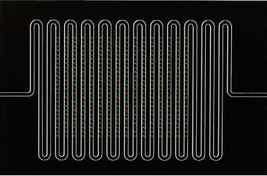
Meandering microfluidic channels with fluorescing pre-immobilized oligonucleotides demonstrate the ability of performing structured functionalization, immobilization of analytes prior to flow cell bonding
(courtesy of Dr. Tobias Bauert, IMT AG, Switzerland).
Lithographic techniques with surface functionalization
Electron beam lithography (EBL) with selective surface chemistry
- Process: EBL patterns sub-10 nm features on a resist-coated substrate. Following development, capture chemistries are applied selectively to exposed areas via self-assembled monolayers (SAMs) or targeted chemical reactions, concluding with a lift-off step to remove residual resist.
- Advantages: Exceptional resolution and capacity for intricate, dense designs.
- Considerations: Low throughput and high cost limit scalability for mass production. Provided the expensive master has been generated, a multi-master approach can enable low-cost pattern generation, e.g., <€40/200mm or 300mm wafer. Though overlay requirements are lower to semicon processes, each specific capture chemistry requires its own lithography step, i.e., production costs are proportional to the number of analytes to be captured.
Nanoimprint lithography (NIL) with sequential functionalization
- Process: Mechanically transfers nanoscale patterns, activates surfaces chemically, and sequentially applies capture chemistries with masking for selective functionalization.
- Advantages: High throughput suitable for larger-scale production and high resolution.
- Considerations: Demands precise alignment and involves complex, multi-step processing similar to the lithographic processes.
Integration of lithography with chemical vapor deposition (CVD)
Combining lithography with CVD techniques allows for precise functional material deposition on micro and nanoscale features.
Selective area CVD:-
- Process: Lithography creates resist patterns, followed by CVD deposition confined to exposed areas. The final step involves resist removal to reveal the patterned functional layers.
- Advantages: Ensures uniform, conformal coatings critical for device consistency and is scalable for wafer-level processing.
- Challenges: Material compatibility and the high temperatures required can affect substrates or reduce bioactivity.
CVD benefits and challenges:
-
-
Uniformity and functionality: Produces consistent thin films with customizable surface properties.
-
Constraints: High operational costs and temperature sensitivity of materials.
-
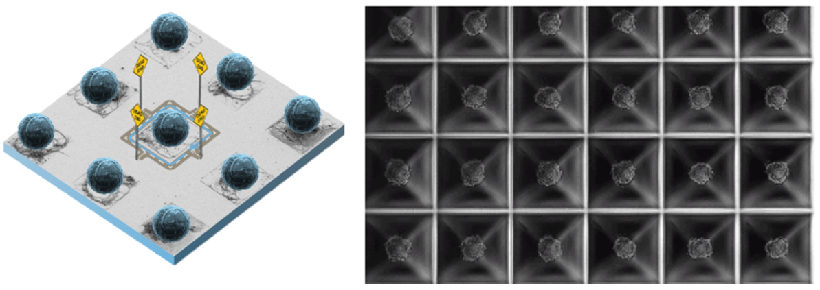
A compelling demonstration of this approach is presented by AlOmier et al. 2025. The authors showcase how photolithography combined with CVD techniques can be used to fabricate microfluidic devices with a precisely controlled spatial distribution of mixed wettability. The study introduces an innovative method for producing micromodels by leveraging photolithographic patterning alongside molecular vapor deposition of perfluorodecyltrichlorosilane. To validate the effectiveness of this fabrication strategy, the researchers conducted two-phase flow experiments supported by numerical simulations (AlOmier et al. 2025).
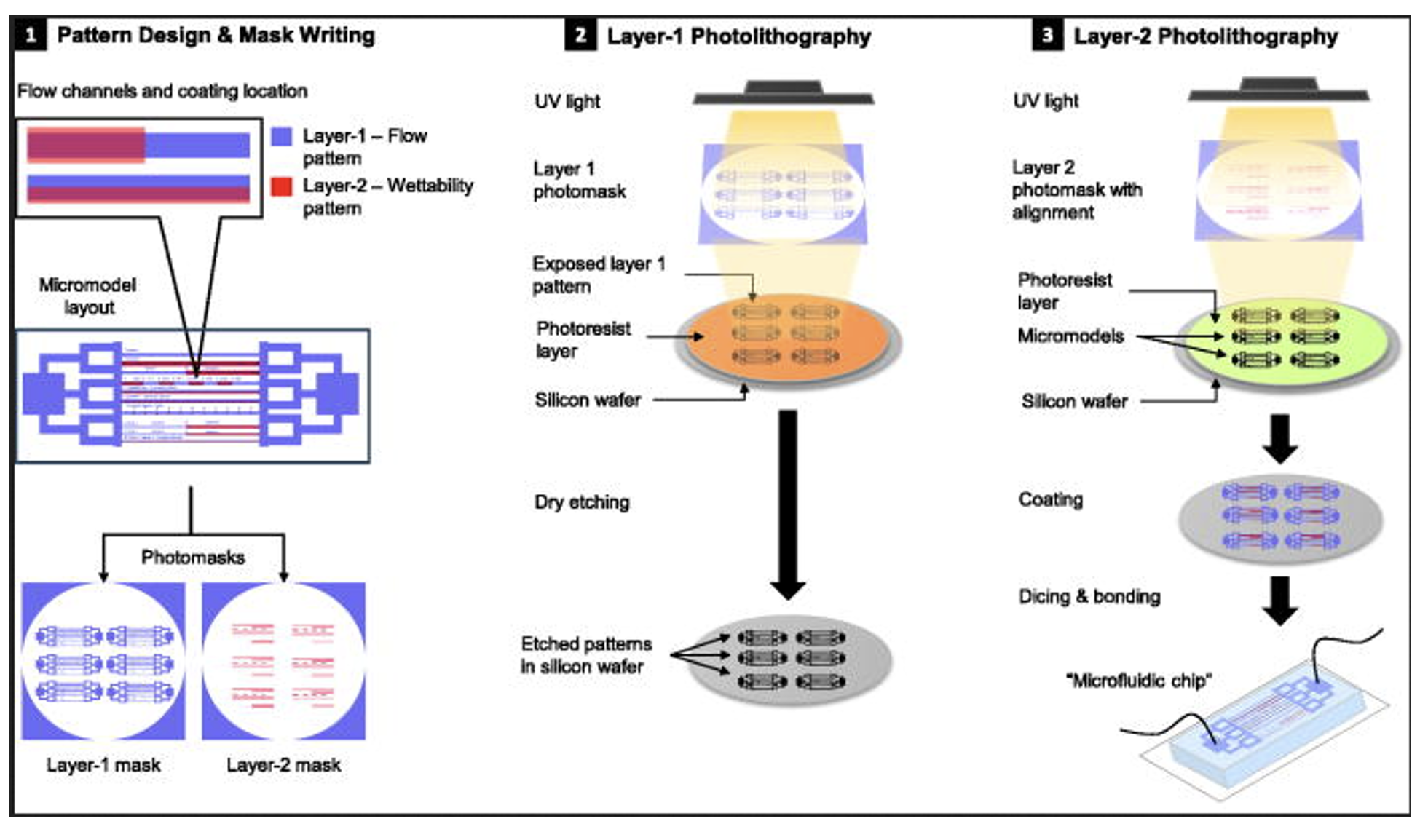
Workflow of the mixed-wettability microfluidics device fabrication process, beginning with (1) pattern design and mask writing, displaying the top view of the entire micromodel layout, sized 2 × 1 cm2 on a 5-inch photomask. This is followed by (2) the first layer of photolithography and dry etching to engrave the flow pattern onto the silicon surface, and (3) the second layer of photolithography with selective coating guided by the second photomask to instill mixed wettability features. The process concludes with the dicing and bonding of the microfluidic devices (from AlOmier et al. 2025).
Advanced biosensing and diagnostics rely on structured surface functionalization with sub-micron precision.
Direct patterning and surface chemistry integration
Inkjet and aerosol jet printing
Direct patterning methods enable the deposition of capture chemistries without the need for masks or resists, offering flexibility and adaptability for various applications.
a. Inkjet printing for biomolecule deposition
-
-
Process:
- Printing: Use inkjet printers to deposit picoliter droplets of capture chemistries onto specific locations on the substrate.
- Spot size control: Adjust droplet volume and substrate properties to achieve spot sizes down to 10 microns; with optimization, potentially around 1 micron.
-
-
-
Advantages:
- Flexibility: Digital, maskless process allows for easy pattern changes and customization.
- Material versatility: Capable of handling various biomolecules, including proteins and nucleic acids.
-
-
-
Considerations:
- Resolution limitations: Achieving 1-micron spots is challenging due to droplet spreading and satellite droplets.
- Surface preparation: May require surface treatments to prevent spreading and improve feature definition.
-
b. Aerosol jet printing for high-resolution patterns
-
-
Process:
- Deposition: Generate an aerosol mist of the capture chemistry solution and focus it onto the substrate.
- Fine feature sizes: Capable of producing features as small as 10 microns, with potential for smaller sizes through optimization.
-
-
-
Advantages:
- Higher resolution: Offers better resolution than traditional inkjet printing, approaching sub-micron scales.
- Non-contact: Reduces the risk of contamination and damage to sensitive substrates.
-
-
-
Considerations:
- Process optimization: Requires fine-tuning of parameters such as aerosol flow rates and substrate temperature.
- Equipment cost: Higher than standard inkjet printers, which may impact scalability.
-
Case Study: Aerosol Jet Printing for Structured Wettability
A recent study by Yaw Akuoko et al. (2024) demonstrates a precise method for selective wettability patterning using aerosol jet printing. By depositing atomized hydrophobic silica nanoparticle droplets onto targeted regions, researchers created well-defined hydrophobic lines with an average width of 60 μm and thickness of 1.32 μm. Overlapping these lines produced superhydrophobic surfaces with a water contact angle of 154°. This technique enables mask-free, material-efficient fabrication of controlled wettability patterns, offering significant potential for microfluidics, cell microarrays, droplet manipulation, and on-target waterproofing of sensitive electronics.
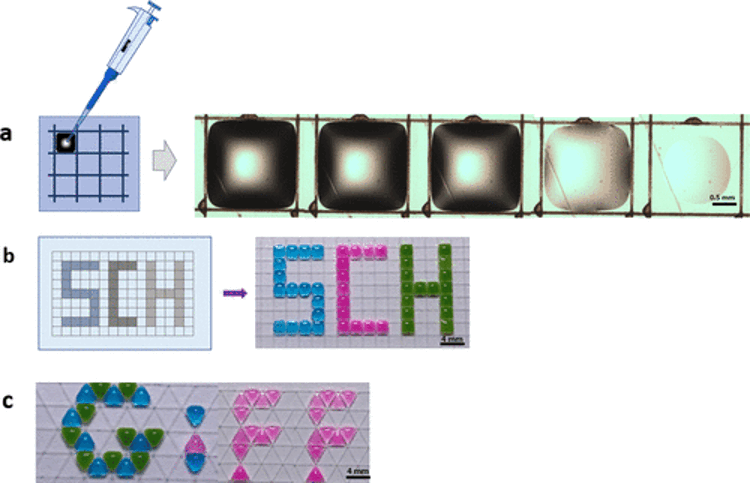
Demonstration of selective wettability for digital patterning. (a) Confinement and evaporation of water drops within the hydrophobic-walled grid. (b) A selectively formed wetting/nonwetting grid using the AJP printing. The grid consists of hydrophilic glass regions (square centers) and hydrophobic boundaries (straight lines); this was used to pattern the letters “SCH”. (c) Photograph of a triangular grid used to create an aesthetic writing (GIFF), by placing colored water droplets on the hydrophilic regions (from Yaw Akuoko et al. 2024).
Combining direct-write methods with surface chemistry strategies
Integrating direct-write techniques with advanced surface chemistry can effectively achieve sub-micron spots with different chemistries, enhancing the functionality of biosensors.
Challenges and considerations
Achieving sub-micron resolution
- Droplet-based methods: Techniques like inkjet and aerosol jet printing face challenges such as droplet spreading and the formation of satellite droplets, which can blur features. Surface treatments (e.g., hydrophobic coatings) can help minimize these effects.
- Material compatibility: Direct-write surface functionalization depends heavily on the compatibility of the material with the functionalization method.
- Capture chemistries: The biological activity of capture molecules must be preserved throughout the patterning process. Exposure to harsh chemicals or high temperatures can deactivate these molecules.
- Process conditions: Selecting materials and processes that are compatible with both the substrate and the capture chemistries is crucial for device functionality.
Throughput and scalability
- Serial processes: Techniques like EBL and DPN are time-consuming and less suited for mass production due to their serial nature.
- Parallel processes: Methods such as NIL and photolithography are more scalable for large-scale production, offering a balance between resolution and throughput.
Multiplexing different chemistries
- Sequential functionalization: Applying different chemistries one after another increases the number of process steps and complexity.
- Parallel functionalization: Using arrays of tools (e.g., multiple AFM tips or printheads) allows for the simultaneous deposition of different chemistries, improving efficiency.
Surface preparation
- Uniformity: A consistent and clean substrate surface is essential for reliable functionalization and reproducible results.
- Activation: Surface treatments like plasma activation may enhance the binding efficiency of capture molecules, improving sensor performance.
Case Study: Maskless Microplasma Surface Patterning for Microfluidics
A novel approach by Wang et al. 2023 leverages microplasma writing to achieve highly localized control of surface wettability without the need for traditional masking techniques. In this study, researchers directly patterned hydrophobic and hydrophilic regions onto PVDF filter paper, enabling precise manipulation of fluid flow in microfluidic devices. The process eliminates predesigned templates, reducing material waste and simplifying fabrication while maintaining high pattern resolution.
This versatile method holds strong potential for applications in lab-on-a-chip systems, point-of-care diagnostics, and other areas where spatially controlled surface chemistry is critical and shows great potential for simple, fast, environmentally friendly and low-cost construction of paper-based microfluidic analytical devices (μPADs).
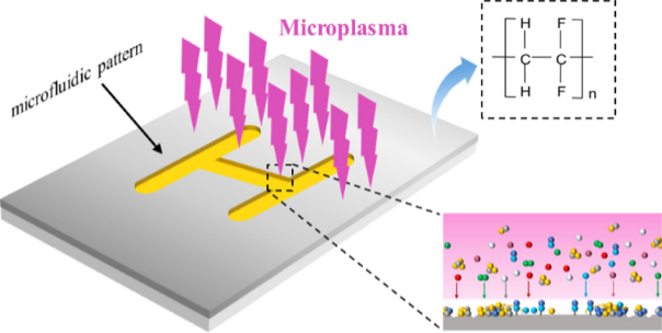
Figure from Wang et al. 2023.
Challenges and solutions in surface functionalization
Effective multiplex detection requires surfaces that enable selective and sensitive binding of different analytes.
Two approaches address these needs:
1. Porous silicon (PSi) and chemical patterning (Zhu et al. 2014)
- Advantages:
-
High surface area: PSi offers a large surface area, increasing the number of available binding sites.
-
Tunable optical properties: The porous structure allows for adjustments in optical characteristics, beneficial for sensor applications.
-
- Techniques:
-
Chemical patterning: Using photolithography and click chemistry to selectively modify surface regions with different functionalities.
-
- Challenges:
-
Uniformity: Maintaining consistent optical properties across the PSi surface can be difficult due to variations in porosity.
-
Non-specific adsorption: Preventing unwanted protein binding that can interfere with analyte detection.
-
- Solutions:
-
Surface modifications: Techniques like hydrosilylation and advanced cleaning processes enhance functionalization consistency and reduce non-specific interactions.
-
Case Study: Porous Silicon (PSi) Chemical Patterning for Multiplex Biosensing
In this study by Zhu et al. 2014, porous silicon (PSi) photonic crystals were functionalized using a combination of photolithography and click chemistry to create spatially controlled chemical patterns for multiplex protease detection. Alkyne-terminated monolayers were applied to the PSi rugate filters, and two distinct ethylene glycol moieties with different terminal groups were selectively conjugated to discrete surface areas via click reactions. To demonstrate targeted biomolecule immobilization, fluorescein isothiocyanate-labeled bovine serum albumin (FITC-BSA) was patterned on the functionalized regions, with fluorescence microscopy confirming selective positioning.
Furthermore, optical reflectivity measurements monitored the chemical functionalization steps and subsequent gelatin immobilization. The platform enabled multiplex detection of protease activity: digestion of gelatin by subtilisin caused measurable blue shifts in the reflectivity spectra at precisely defined surface positions. This precise spatial control makes PSi photonic crystals a promising microarray platform for high-throughput biosensing and cell-based assay applications.
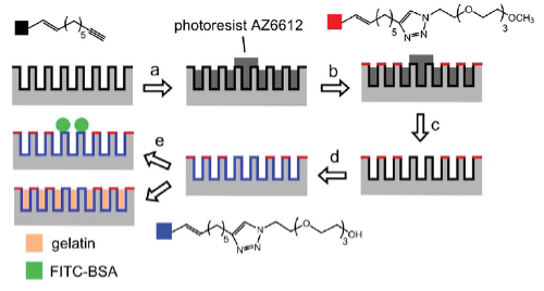
Procedure for the patterning of discrete functionalities to PSi surface by a combination of photolithography of photoresist and click chemistry. Freshly etched PSi rugate filter was firstly functionalized with an alkyne-terminated monolayer. (a) An array of photoresist circles with diameter 100 mm was patterned on the PSi surface by photolithography. (b) The first azido species azido-EO3–OCH3 was attached on the upper region of pore structure in background regions by a click reaction with only water as the solvent. (c) Photoresist pattern was removed completely by rinsing the chip with acetone and isopropanol. (d) The second azido species azido-EO3–OH was attached on the surface of spot regions and throughout the internal pore walls of the entire structure. (e) FITC-BSA was attached on chemically patterned PSi surface for fluorescence microscopy, or gelatin was filled in the internal pore space of the entire structure for protease assay (from Zhu et al. 2014).
Effective multiplex detection requires surfaces that selectively and sensitively bind different analytes.
2. Plasmonic biosensors
-
Advantages:
-
Sensitive detection: Relies on the interaction of light with metal surfaces to detect binding events with high sensitivity.
-
Real-time monitoring: Capable of observing interactions as they occur, providing immediate feedback.
-
-
Techniques:
-
Precise functionalization: Utilize self-assembled monolayers (SAMs) and site-specific coupling to immobilize capture molecules accurately.
-
-
Challenges:
-
Cross-talk: Preventing interference between adjacent functionalized regions is critical for multiplexing.
-
Scalability: Difficulties in scaling precise functionalization methods for mass production.
-
-
Solutions:
-
Orthogonal functionalization strategies: Employing chemical techniques that allow different capture chemistries to coexist without interference.
-
Surface coatings: Using materials like polyethylene glycol (PEG) to reduce non-specific adsorption and enhance overall performance.
-
Recommendations
- High resolution and precision
- Electron beam lithography with selective chemistry: Ideal for applications where ultra-high precision is essential, despite higher costs and lower throughput.
- Dip-pen nanolithography: Suitable for depositing sensitive biological molecules at the nanoscale, particularly in research and development settings.
- Scalability and throughput
- Nanoimprint lithography with sequential functionalization: Balances high resolution with improved throughput, making it more suitable for larger-scale production.
- Photolithography combined with microfluidics: Offers scalability for features around 1 micron, suitable for batch processing and mass production.
- Flexibility and rapid prototyping
- Inkjet or aerosol jet printing: Excellent for rapid iteration and customization, with potential for micron-scale features. Ideal for exploratory research and small-scale production.
- Laser direct-write methods: Allow for maskless patterning with reasonable resolution, offering flexibility for design changes without the need for new masks.
- Combining techniques
- Hybrid approaches: Utilize lithography for defining high-resolution patterns and direct-write methods to selectively deposit capture chemistries, leveraging the strengths of each technique.
- Surface modification: Employ CVD or other chemical treatments to alter surface properties, enhancing the effectiveness and specificity of direct patterning methods.
The essence of this article
Creating structured surface functionalization with micron or sub-micron spots bearing different capture chemistries is achievable through a variety of methods. The choice of technique depends on specific requirements such as resolution, throughput, material compatibility, and cost considerations.
- Lithographic techniques offer the highest resolution and are suitable when precision is critical, despite higher complexity and expense.
- Direct patterning methods provide flexibility and ease of use, making them ideal for rapid prototyping and applications where ultra-high resolution is not mandatory.
- Combination approaches integrating multiple methods can achieve both high resolution and functional versatility, optimizing performance and efficiency.
By carefully selecting and optimizing manufacturing methods and surface functionalization techniques, it is possible to fabricate surfaces with precisely patterned capture chemistries.
The future of microfluidics
The advancement of multiplexed analyte detection in microfluidic systems holds immense potential for diagnostics. These platforms offer high-throughput, sensitive, and cost-effective solutions suitable for both clinical and research applications. While challenges in fabrication, sensitivity, and user-friendliness exist, ongoing innovations – particularly in patient-centric and wearable diagnostics — are overcoming these hurdles.
To ensure that these technologies successfully migrate from research prototypes to real-world, on-site diagnostics (xPOCT), future efforts must integrate high-level multiplexing strategies with ease of operation and minimal external instrumentation. The examples of mChip, DxBox, and MultiLab highlight ongoing progress, but also show that balancing system complexity with user-friendliness is still a challenge. Overall, combining robust manufacturing methods, stable reagent storage, and well-validated assay designs can help these multiplexed microfluidic devices find broader acceptance across clinical and resource-limited settings alike.
This capability is crucial for advanced analyte detection, contributing to the development of more sensitive, specific, and multiplexed biosensors. Such advancements hold significant promise for improving diagnostics, personalized medicine, and a wide range of applications in healthcare and environmental monitoring.
Missed the first two parts of this series?
Read Alexis’ insightful articles:
- Microfluidics in Focus: Benefits and Breakthroughs
- Microfluidics in Focus: Materials that Matter
- Microfluidics in Focus: From Design to Device
This is the final part of this blog series.
Follow us on LinkedIn and be the first to know about our new blog articles!
We support your success
As a global systems engineering provider with a proven track record in life science and diagnostics, we recognize your need for innovative solutions. Our deep microfluidics expertise, combined with a full understanding of your workflows, enables us to transform your vision into market-ready solutions that exceed customer expectations.
Contact us and discover how we can help you innovate faster and smarter.

Microfluidics Expert Alexis Tzannis
Alexis holds a PhD in physical chemistry from ETH Zürich, is fluent in four languages, and has a proven record of forging academia–industry partnerships to accelerate innovation. A founding member of the Microfluidics Association (MFA), he is a micro- and nanotechnology business leader with 15 years of experience taking microfluidic products from concept to industrialization.
Alexis has delivered double-digit sales growth at HSE•AG and previously at IMT Microtechnologies by leading cross-functional teams and cultivating global key accounts. His technical expertise spans the design and manufacture of glass, silicon, and hybrid-material microfluidic platforms that enable cutting-edge analytical applications, e.g., next-generation sequencing (NGS) and others.